What is a Switch Mode Power Supply?
To understand why electronic evolution has led to a much more complicated way of making regulated power supply units (PSU from here on), we need to go back a bit and look at linear PSU’s. These were simple, reliable, quiet PSUs with good regulation and low ripple—so why change?

There are two main reasons, and both relate to cost.
As the transformer operates at a mains frequency of 50 or 60 Hz, the core needs to be large as its cross-section is a function of frequency. This means a large block of steel and copper, all rather pricey today. Secondly, the regulating series pass transistor will always have a linear voltage between its input and output. This multiplied by the current is the power that needs to be gotten rid of as heat, requiring a large and expensive aluminum heat sink.
For example, a 50V variable PSU set to 5V and delivering 2A might have (50-5)*2 = 90W of heat to dissipate. A Switched Mode Power Supply (SMPS from here on) nearly eliminates both of these issues at the expense of circuit complexity by increasing the transformer frequency to make it smaller and seeing that the regulator device is always fully on or fully off thus dissipating much less heat.
How an SMPS Works
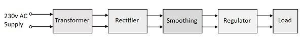
In the block diagram above, the mains are fed directly into the first block without using a transformer. Of course, diodes and capacitors used here must be up to the job. Note that DC could also be fed here, for example, in a 12 to 5V DC to DC converter. The incoming AC mains is now a rectified DC at high voltage.
The next block is the high-frequency converter, a chopper circuit turning a power device such as a MOSFET on and off at several kHz. This is converting the incoming DC to a square wave fed to a suitably designed high-frequency transformer with a secondary at a voltage suitable for the output voltage we want. This transformer also provides galvanic isolation between the output voltage and the incoming mains or DC.
The next stage once again rectifies this and filters out ripple and noise. The last block, the control circuit, is where the magic happens. This is a feedback circuit controlling the chopper MOSFET.
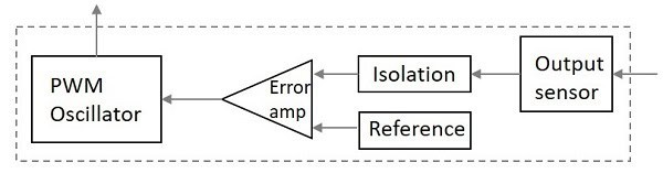
The control circuit has a voltage divider/multiplier that senses the output voltage. Because we will feed this back to the chopper circuit running at hundreds of volts, it needs to be isolated, usually with an optocoupler. There is a reference—it could be a fixed reference diode or a trimpot. The error amp compares these two voltages and adjusts the PWM (pulse width modulation) oscillator, which controls the MOSFET.
Putting it all together
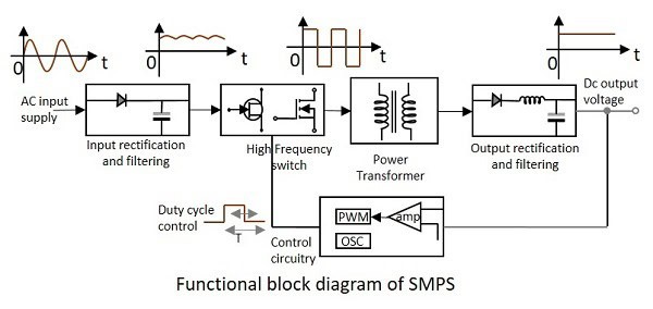
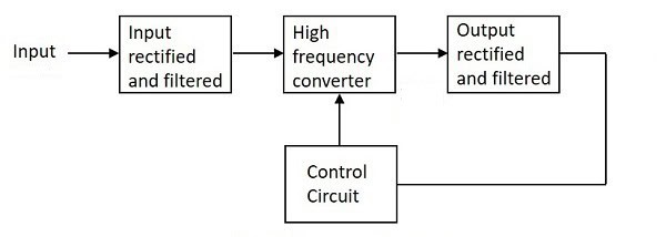
The functional block diagram above gives a better and more detailed look at the parts involved.
Practical Example
Shown below is a straightforward yet working example compared to the monster you may find inside your PC power supply> It will demonstrate the principle we discussed above.

All the complex functions of the PWM generator, MOSFET chopper switch, and error and control are taken care of in one IC, the TNY267. The final output is 12V, and it can deliver 1A.
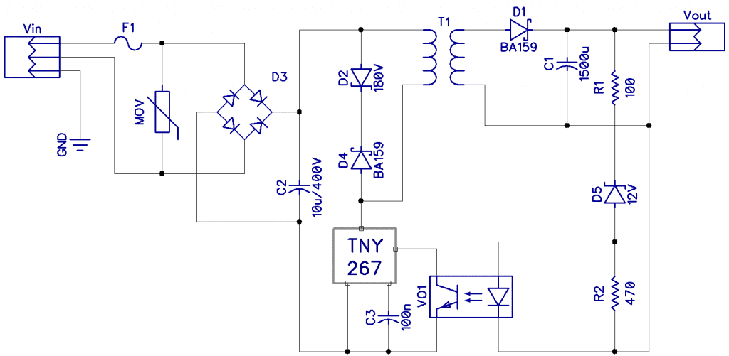
From left to right, Vin is the 100-300V AC mains or even a DC source. The MOV is a type of resistor that goes short circuit on a high voltage spike over 275V and blows the fuse F1, but F1 is slow acting and can withstand the initial inrush current of the circuit. D3 is a full-wave bridge rectifier, and the DC output appears across C2. For a 220V input, this would be about 220*1.4 = 308V, so be aware!
The TNY runs at about 132kHz. D2 is a 180V transient suppression diode to handle back EMF spikes.
D1 (Schottky) on the secondary rectifies the 132kHz AC, and C1 smooths and kills ripple. C3 is a required bypass cap. R1, R2, and D5 provide a feedback circuit to the TNY via an optoisolator to ensure we have galvanic isolation from the mains at all points.
As many of these components are working hard, care must be taken in their selection, like the voltage, equivalent series resistance, etc.

The primary of T1 is 157t, and the secondary is 14t. The core is an E19 type ferrite transformer with a central core of about 4.5×4.5mm.
Now, we know how much more efficient an SMPSU can be, yet it is more complex and requires quality components for reliability.
Permission to use some images from www.tutorialspoint.com.