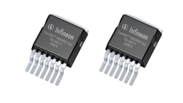
Infineon introduces CoolSiC™ MOSFET G2
The next generation of silicon carbide technology for high-performance systems that drive decarbonization
Munich, Germany – March 5, 2024 – Infineon Technologies AG (FSE: IFX / OTCQX: IFNNY) opens a new chapter in power systems and energy conversion and introduces the next generation of silicon carbide (SiC) MOSFET trench technology. The new Infineon CoolSiC™ MOSFET 650 V and 1200 V Generation 2 improve MOSFET key performance figures such as stored energies and charges by up to 20 percent compared to the previous generation without compromising quality and reliability levels leading to higher overall energy efficiency and further contributing to decarbonization.

CoolSiC MOSFET Generation 2 (G2) technology continues to leverage performance capabilities of silicon carbide by enabling lower energy loss that turns into higher efficiency during power conversion. This provides strong benefits to customers for various power semiconductor applications such as photovoltaics, energy storage, DC EV charging, motor drives and industrial power supplies. A DC fast charging station for electric vehicles which is equipped with CoolSiC G2 allows for up to 10 percent less power loss compared to previous generations, while enabling higher charging capacity without compromising form factors. Traction inverters based on CoolSiC G2 devices can further increase electric vehicle ranges. In the area of renewable energies, solar inverters designed with CoolSiC G2 make smaller sizes possible while maintaining a high power output, resulting in a lower cost per watt.
“Megatrends call for new and efficient ways to generate, transmit and consume energy. With the CoolSiC MOSFET G2, Infineon brings silicon carbide performance to a new level,” said Dr. Peter Wawer, Division President Green Industrial Power at Infineon. “This new generation of SiC technology enables the accelerated design of more cost-optimized, compact, reliable, and highly efficient systems harvesting energy-savings and reducing CO 2 for every watt installed in the field. It’s a great example of Infineon’s relentless spirit, constantly pushing for innovation to drive decarbonization and digitalization in the industrial, consumer and automotive sectors.”
Contributing to high-performance CoolSiC G2 solutions, Infineon’s pioneer CoolSiC MOSFET trench technology provides an optimized design trade-off, allowing higher efficiency and reliability compared to SiC MOSFET technology available so far. Combined with the award-winning .XT packaging technology, Infineon is further increasing the potential of designs based on CoolSiC G2 with higher thermal conductivity, better assembly control and improved performance.
Mastering all relevant power technologies in silicon, silicon carbide and gallium nitride (GaN), Infineon offers design flexibility and leading-edge application know-how that meet the expectations and demands of modern designers. Innovative semiconductors based on wide-bandgap (WBG) materials like SiC and GaN are the key to conscious and efficient use of energy in fostering decarbonization.
Register here for the online media briefing (5 March, 10 AM CET) and learn more about Infineon’s CoolSiC MOSFET 650 V and 1200 V G2.
Join us at the 2024 Infineon Wide-Bandgap Developer Forum on 16 April. Register here.

